IC
IC


Erasable Programmable Read-Only Memory (EPROM) integrated circuits. These packages have a transparent window that shows the die inside. The window is used to erase the memory by exposing the chip to ultraviolet light.

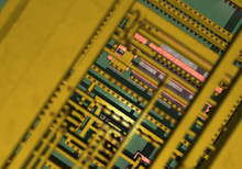
Integrated circuit from an EPROM memory microchip showing the memory blocks, the supporting circuitry and the fine silver wires which connect the integrated circuit die to the legs of the packaging.

Synthetic detail of an integrated circuit through four layers of planarized copper interconnect, down to the polysilicon (pink), wells (greyish), and substrate (green)
An integrated circuit or monolithic integrated circuit (also referred to as an IC, a chip, or amicrochip) is a set of electronic circuits on one small flat piece (or "chip") ofsemiconductor material, normally silicon. The integration of large numbers of tinytransistors into a small chip results in circuits that are orders of magnitude smaller, cheaper, and faster than those constructed of discreteelectronic components. The IC's mass production capability, reliability and building-block approach to circuit design has ensured the rapid adoption of standardized ICs in place of designs using discrete transistors. ICs are now used in virtually all electronic equipment and have revolutionized the world of electronics. Computers, mobile phones, and other digital home appliances are now inextricable parts of the structure of modern societies, made possible by the small size and low cost of ICs.
ICs were made possible by experimental discoveries showing that semiconductor devices could perform the functions ofvacuum tubes, and by mid-20th-century technology advancements in semiconductor device fabrication. Since their origins in the 1960s, the size, speed, and capacity of chips have progressed enormously, driven by technical advances that fit more and more transistors on chips of the same size - a modern chip may have several billiontransistors in an area the size of a human fingernail. These advances, roughly followingMoore's law, make a computer chip of today possess millions of times the capacity and thousands of times the speed of the computer chips of the early 1970s.
ICs have two main advantages over discrete circuits: cost and performance. Cost is low because the chips, with all their components, are printed as a unit by photolithographyrather than being constructed one transistor at a time. Furthermore, packaged ICs use much less material than discrete circuits. Performance is high because the IC's components switch quickly and consume comparatively little power because of their small size and close proximity. The main disadvantage of ICs is the high cost to design them and fabricate the required photomasks. This high initial cost means ICs are only practical when high production volumes are anticipated.
Terminology
Circuits meeting this definition can be constructed using many different technologies, including thin-film transistors,thick film technologies, or hybrid integrated circuits. However, in general usage integrated circuit has come to refer to the single-piece circuit construction originally known as amonolithic integrated circuit.[2][3]
Invention
Early developments of the integrated circuit go back to 1949, when German engineerWerner Jacobi (Siemens AG)[4] filed a patent for an integrated-circuit-like semiconductor amplifying device[5] showing five transistors on a common substrate in a 3-stage amplifierarrangement. Jacobi disclosed small and cheap hearing aids as typical industrial applications of his patent. An immediate commercial use of his patent has not been reported.
The idea of the integrated circuit was conceived by Geoffrey Dummer (1909–2002), a radar scientist working for the Royal Radar Establishment of the British Ministry of Defence. Dummer presented the idea to the public at the Symposium on Progress in Quality Electronic Components inWashington, D.C. on 7 May 1952.[6] He gave many symposia publicly to propagate his ideas and unsuccessfully attempted to build such a circuit in 1956.
A precursor idea to the IC was to create small ceramic squares (wafers), each containing a single miniaturized component. Components could then be integrated and wired into a bidimensional or tridimensional compact grid. This idea, which seemed very promising in 1957, was proposed to the US Army by Jack Kilby and led to the short-lived Micromodule Program (similar to 1951's Project Tinkertoy).[7] However, as the project was gaining momentum, Kilby came up with a new, revolutionary design: the IC.

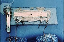
Jack Kilby's original integrated circuit
Newly employed by Texas Instruments, Kilby recorded his initial ideas concerning the integrated circuit in July 1958, successfully demonstrating the first working integrated example on 12 September 1958.[8] In his patent application of 6 February 1959,[9] Kilby described his new device as "a body of semiconductor material … wherein all the components of the electronic circuit are completely integrated."[10] The first customer for the new invention was the US Air Force.[11]
Kilby won the 2000 Nobel Prize in Physics for his part in the invention of the integrated circuit.[12] His work was named an IEEE Milestone in 2009.[13]
Half a year after Kilby, Robert Noyce atFairchild Semiconductor developed his own idea of an integrated circuit that solved many practical problems Kilby's had not. Noyce's design was made of silicon, whereas Kilby's chip was made of germanium. Noyce creditedKurt Lehovec of Sprague Electric for the principle of p–n junction isolation, a key concept behind the IC.[14] This isolation allows each transistor to operate independently despite being parts of the same piece of silicon.
Fairchild Semiconductor was also home of the first silicon-gate IC technology with self-aligned gates, the basis of all modern CMOScomputer chips. The technology was developed by Italian physicist Federico Fagginin 1968. In 1970, he joined Intel in order to develop the first single-chip central processing unit (CPU) microprocessor, theIntel 4004, for which he received the National Medal of Technology and Innovation in 2010. The 4004 was designed by Busicom'sMasatoshi Shima and Intel's Ted Hoff in 1969, but it was Faggin's improved design in 1970 that made it a reality.[15]
Advances
Advances in IC technology, primarily smaller features and larger chips, have allowed the number of transistors in an integrated circuit to double every two years, a trend known asMoore's law. This increased capacity has been used to decrease cost and increase functionality. In general, as the feature size shrinks, almost every aspect of an IC's operation improves. The cost per transistor and the switching power consumption per transistor go down, while the memory capacity and speed go up, through the relationships defined by Dennard scaling.[16]Because speed, capacity, and power consumption gains are apparent to the end user, there is fierce competition among the manufacturers to use finer geometries. Over the years, transistor sizes have decreased from 10s of microns in the early 1970s to 10nanometers in 2017 [17] with a corresponding million-fold increase in transistors per unit area. As of 2016, typical chip areas range from a few square millimeters to around 600 mm2, with up to 25 million transistors per mm2.[18]
The expected shrinking of feature sizes, and the needed progress in related areas was forecast for many years by the International Technology Roadmap for Semiconductors(ITRS). The final ITRS was issued in 2016, and it is being replaced by the International Roadmap for Devices and Systems.[19]
Initially, ICs were strictly electronic devices. The success of ICs has led to the integration of other technologies, in the attempt to obtain the same advantages of small size and low cost. These technologies include mechanical devices, optics, and sensors.
- Very small mechanical devices driven by electricity can be integrated onto chips, a technology known asmicroelectromechanical systems. These devices were developed in the late 1980s[20]and are used in a variety of commercial and military applications. Examples include DLP projectors, inkjet printers, andaccelerometers and MEMS gyroscopesused to deploy automobile airbags.
- Since the early 2000s, the integration of optical functionality (optical computing) into silicon chips has been actively pursued in both academic research and in industry resulting in the successful commercialization of silicon based integrated optical transceivers combining optical devices (modulators, detectors, routing) with CMOS based electronics.[21]Integrated optical circuits are also being developed.
- Integrated circuits are also being developed for sensor applications in medical implantsor other bioelectronic devices.[22] Special sealing techniques have to be applied in such biogenic environments to avoidcorrosion or biodegradation of the exposed semiconductor materials.[23]
As of 2016, the vast majority of all transistors are fabricated in a single layer on one side of a chip of silicon in a flat 2-dimensional planar process. Researchers have produced prototypes of several promising alternatives, such as:
- various approaches to stacking several layers of transistors to make a three-dimensional integrated circuit, such asthrough-silicon via, "monolithic 3D",[24]stacked wire bonding,[25] etc.
- transistors built from other materials:graphene transistors, molybdenite transistors, carbon nanotube field-effect transistor, gallium nitride transistor, transistor-like nanowire electronic devices,organic field-effect transistor, etc.
- fabricating transistors over the entire surface of a small sphere of silicon.[26][27]
- modifications to the substrate, typically to make "flexible transistors" for a flexible display or other flexible electronics, possibly leading to a roll-away computer.
Design
The cost of designing and developing a complex integrated circuit is quite high, normally in the multiple tens of millions of dollars.[28] This only makes economic sense if production volume is high, so the non-recurring engineering (NRE) costs are spread across typically millions of production units.
Modern semiconductor chips have billions of components, and are too complex to be designed by hand. Software tools to help the designer are essential. Electronic Design Automation (EDA), also referred to as Electronic Computer-Aided Design (ECAD),[29]is a category of software tools for designingelectronic systems, including integrated circuits. The tools work together in a design flow that engineers use to design and analyze entire semiconductor chips.
Types

Integrated circuits can be classified intoanalog,[30] digital[31] and mixed signal[32] (both analog and digital on the same chip).
Digital integrated circuits can contain anywhere from one[33] to billions[18] of logic gates, flip-flops, multiplexers, and other circuits in a few square millimeters. The small size of these circuits allows high speed, low power dissipation, and reducedmanufacturing cost compared with board-level integration. These digital ICs, typicallymicroprocessors, DSPs, and microcontrollers, work using boolean algebra to process "one" and "zero" signals.

Among the most advanced integrated circuits are the microprocessors or "cores", which control everything from computers and cellular phones to digital microwave ovens. Digital memory chips and application-specific integrated circuits (ASICs) are examples of other families of integrated circuits that are important to the modern information society.
In the 1980s, programmable logic deviceswere developed. These devices contain circuits whose logical function and connectivity can be programmed by the user, rather than being fixed by the integrated circuit manufacturer. This allows a single chip to be programmed to implement different LSI-type functions such as logic gates, addersand registers. Current devices called field-programmable gate arrays (FPGAs) can (as of 2016) implement the equivalent of millions of gates in parallel and operate up to 1 GHz.[34]
Analog ICs, such as sensors, power management circuits, and operational amplifiers, work by processing continuous signals. They perform functions likeamplification, active filtering, demodulation, and mixing. Analog ICs ease the burden on circuit designers by having expertly designed analog circuits available instead of designing a difficult analog circuit from scratch.
ICs can also combine analog and digital circuits on a single chip to create functions such as A/D converters and D/A converters. Such mixed-signal circuits offer smaller size and lower cost, but must carefully account for signal interference. Prior to the late 1990s, radios could not be fabricated in the same low-cost CMOS processes as microprocessors. But since 1998, a large number of radio chips have been developed using CMOS processes. Examples include Intel's DECT cordless phone, or 802.11 (Wi-Fi) chips created by Atheros and other companies.[35]
Modern electronic component distributorsoften further sub-categorize the huge variety of integrated circuits now available:
- Digital ICs are further sub-categorized as logic ICs, memory chips, interface ICs (level shifters, serializer/deserializer, etc.), Power Management ICs, and programmable devices.
- Analog ICs are further sub-categorized as linear ICs and RF ICs.
- mixed-signal integrated circuits are further sub-categorized as data acquisition ICs (including A/D converters, D/A converter,digital potentiometers) and clock/timing ICs.
Manufacturing
Intellectual property
The possibility of copying by photographing each layer of an integrated circuit and preparing photomasks for its production on the basis of the photographs obtained is a reason for the introduction of legislation for the protection of layout-designs. TheSemiconductor Chip Protection Act of 1984established intellectual property protection for photomasks used to produce integrated circuits.[40]
A diplomatic conference was held at Washington, D.C., in 1989, which adopted aTreaty on Intellectual Property in Respect of Integrated Circuits (IPIC Treaty).
Other developments
Generations
Silicon labelling and graffiti
ICs and IC families
- The 555 timer IC
- The 741 operational amplifier
- 7400 series TTL logic building blocks
- 4000 series, the CMOS counterpart to the 7400 series (see also: 74HC00 series)
- Intel 4004, the world's first microprocessor, which led to the famous 8080 CPU and then the IBM PC's 8088, 80286, 486 etc.
- The MOS Technology 6502 and Zilog Z80microprocessors, used in many home computers of the early 1980s
- The Motorola 6800 series of computer-related chips, leading to the 68000 and88000 series (used in some Apple computers and in the 1980s CommodoreAmiga series)
- The LM-series of analog integrated circuits


Comments
Post a Comment